- 您现在的位置:买卖IC网 > Sheet目录323 > DSP56311EVM (Freescale Semiconductor)KIT EVALUATION FOR DSP56311
�� �
�
�ESSI� Programming� Model�
�7.5.7� ESSI� Transmit� Data� Registers� (TX[2–0])�
�ESSI0:TX20,� TX10,� TX00;� ESSI1:TX21,� TX11,� TX01�
�TX2,� TX1,� and� TX0� are� 24-bit� write-only� registers.� Data� written� into� these� registers�
�automatically� transfers� to� the� transmit� shift� registers.� (See� Figure� 7-12� and� Figure� 7-13� .)� The�
�data� transmitted� (8,� 12,� 16,� or� 24� bits)� is� aligned� according� to� the� value� of� the� ALC� bit.� When� the�
�ALC� bit� is� cleared,� the� MSB� is� Bit� 23.� When� ALC� is� set,� the� MSB� is� Bit� 15.� If� the� transmit� data�
�register� empty� interrupt� has� been� enabled,� the� DSP� is� interrupted� whenever� a� transmit� data�
�register� becomes� empty.�
�Note:�
�When� data� is� written� to� a� peripheral� device,� there� is� a� two-cycle� pipeline� delay� while�
�any� status� bits� affected� by� this� operation� are� updated.� If� any� of� those� status� bits� are� read�
�during� the� two-cycle� delay,� the� status� bit� may� not� reflect� the� current� status.�
�7.5.8� ESSI� Time� Slot� Register� (TSR)�
�TSR� is� effectively� a� write-only� null� data� register� that� prevents� data� transmission� in� the� current�
�transmit� time� slot.� For� timing� purposes,� TSR� is� a� write-only� register� that� behaves� as� an� alternative�
�transmit� data� register,� except� that,� rather� than� transmitting� data,� the� transmit� data� signals� of� all� the�
�enabled� transmitters� are� in� the� high-impedance� state� for� the� current� time� slot.�
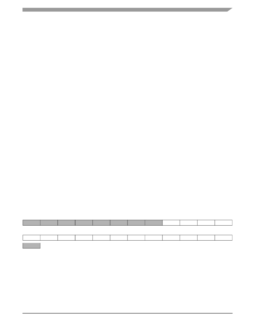
�7.5.9� Transmit� Slot� Mask� Registers� (TSMA,� TSMB)�
�Both� transmit� slot� mask� registers� are� read/write� registers.� When� the� TSMA� or� TSMB� is� read� to�
�the� internal� data� bus,� the� register� contents� occupy� the� two� low-order� bytes� of� the� data� bus,� and� the�
�high-order� byte� is� filled� by� 0.� In� Network� mode� the� transmitter(s)� use� these� registers� to� determine�
�which� action� to� take� in� the� current� transmission� slot.� Depending� on� the� bit� settings,� the�
�transmitter(s)� either� tri-state� the� transmitter(s)� data� signal(s)� or� transmit� a� data� word� and� generate�
�a� transmitter� empty� condition.�
�23�
�22�
�21�
�20�
�19�
�18�
�17�
�16�
�15�
�14�
�13�
�12�
�TS15�
�TS14�
�TS13�
�TS12�
�11�
�TS11�
�10�
�TS10�
�9�
�TS9�
�8�
�TS8�
�7�
�TS7�
�6�
�TS6�
�5�
�TS5�
�4�
�TS4�
�3�
�TS3�
�2�
�TS2�
�1�
�TS1�
�0�
�TS0�
�—Reserved� bit;� read� as� 0;� write� to� 0� 0� for� future� compatibility.�
�(ESSI0� X:$FFFFB4,� ESSI1� X:$FFFFA4)�
�Figure� 7-14.� ESSI� Transmit� Slot� Mask� Register� A� (TSMA)�
�DSP56311� User’s� Manual,� Rev.� 2�
�Freescale� Semiconductor�
�7-31�
�发布紧急采购,3分钟左右您将得到回复。
相关PDF资料
DSPAUDIOEVMMB1E
BOARD MOTHER DSP563XX
DSPIC30F2010 DEVELOPMENT KIT
KIT DEV EMBEDDED C
DSTRM-KT-0181A
DSTREAM DEBUG AND TRACE UNIT
DSUT1CSU
SURGE SUPPR NETWORK W/GROUND
DTEL2
SURGE SUPPRESSOR PHONE RJ11/RJ45
DV003001
PROGRAMMER PICSTART PLUS 16C/17C
DV164035
MPLAB ICD3 IN-CIRC DEBUGGER
DV164039
KIT DEV PIC24FJ256DA210
相关代理商/技术参数
DSP56311EVMIG_D
制造商:未知厂家 制造商全称:未知厂家 功能描述:DSP56311EVMIG DSP56311EVM Sample Code
DSP56311EVMUM
制造商:未知厂家 制造商全称:未知厂家 功能描述:DSP56311 Evaluation Module Hardware Reference Manual
DSP56311FACT
制造商:未知厂家 制造商全称:未知厂家 功能描述:DSP56311 Higher performance programmable DSP for demanding voice and data applications
DSP56311UM
制造商:未知厂家 制造商全称:未知厂家 功能描述:DSP56311 24-Bit Digital Signal Processor Users Manual
DSP56311UMAD
制造商:未知厂家 制造商全称:未知厂家 功能描述:DSP56311 Users Manual Addendum
DSP56311VF150
功能描述:数字信号处理器和控制器 - DSP, DSC 150Mhz/300MMACS 150Mhz EFCOP RoHS:否 制造商:Microchip Technology 核心:dsPIC 数据总线宽度:16 bit 程序存储器大小:16 KB 数据 RAM 大小:2 KB 最大时钟频率:40 MHz 可编程输入/输出端数量:35 定时器数量:3 设备每秒兆指令数:50 MIPs 工作电源电压:3.3 V 最大工作温度:+ 85 C 封装 / 箱体:TQFP-44 安装风格:SMD/SMT
DSP56311VF150B1
功能描述:数字信号处理器和控制器 - DSP, DSC 24 BIT DSP
RoHS:否 制造商:Microchip Technology 核心:dsPIC 数据总线宽度:16 bit 程序存储器大小:16 KB 数据 RAM 大小:2 KB 最大时钟频率:40 MHz 可编程输入/输出端数量:35 定时器数量:3 设备每秒兆指令数:50 MIPs 工作电源电压:3.3 V 最大工作温度:+ 85 C 封装 / 箱体:TQFP-44 安装风格:SMD/SMT
DSP56311VF150R2
功能描述:数字信号处理器和控制器 - DSP, DSC 24 BIT DSP RoHS:否 制造商:Microchip Technology 核心:dsPIC 数据总线宽度:16 bit 程序存储器大小:16 KB 数据 RAM 大小:2 KB 最大时钟频率:40 MHz 可编程输入/输出端数量:35 定时器数量:3 设备每秒兆指令数:50 MIPs 工作电源电压:3.3 V 最大工作温度:+ 85 C 封装 / 箱体:TQFP-44 安装风格:SMD/SMT